Do you encountered any difficulties in processing of high-precision Si mold substrates
(resin molding ~ glass molding), microfluidic chips,microwell plates, medical analysis
and detection boards and the use of MEMS technology?
Please feel free to commission it to CITIZEN FINEDEVICE Co.,LTD..
We provide you with“from trial production to mass production,
from molds to components”one-stop service.

TOP > MEMS
Contact
Inquiry form

What is MEMS?

MEMS (Micro Electro Mechanical Systems) is a component, which is formed by integrating mechanical parts, sensors, actuators and electronic circuits on a silicon substrate, a glass substrate, an organic material or other materials, using the microfabrication technique.
Due to process limitations or different materials, the mechanical structure and the electronic circuit may use different chips. Such hybrid system is also called MEMS.

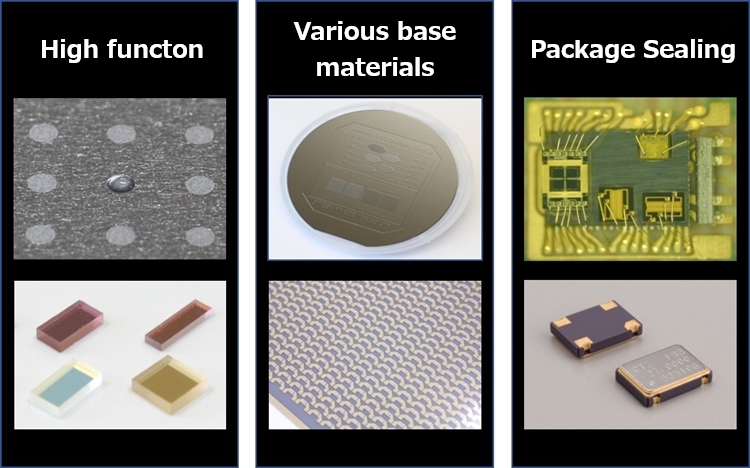
How does CITIZEN FINEDEVICE Co.,LTD. think about MEMS?

Since the MEMS processing technology was created, we have had more than 20 years experience and developed sensor MEMS, actuator MEMS and package MEMS.
Along with the above technology development, we have specialized in the micro-machining technology for substrate materials other than Si (ceramics, glass and crystal) continuously, established relevant systems, utilized crystal oscillator manufacturing technology and established wafer manufacturing process. And we provide services from cutting to packaging.
At present, the company is involved in the fields of electronic parts for people’s life, clock parts and medical industry. It realizes the achievement in mass production of medical detection boards, the realization of which is attributed to our proprietary substrate processing technology, and also reflects the advantages of film forming technology.
In addition to our products, we also have the ability to use MEMS technology and micro machining technology to manufacture precision molds.
In terms of trial production and development in the process, we combine the proprietary technologies to provide the best scheme, and as a wafer foundry, we can achieve one-stop production from wafer processing to packaging to meet the requirements of customers.


The history of MEMS

MEMS began with micro machining in the 1960s.
Strain gauges with the piezoresistive effect of monocrystalline silicon applied were developed around 1970 and used as strain sensors.
After that, isotropic and anisotropic silicon wet etching was developed, and it became possible to form physical structures in addition to piezoresistive elements. It has been used as a pressure sensor for automobiles since the latter half of the 1970s. At present, MEMS components are evolving into components with more complex mechanisms, such as acceleration sensors for automobile airbags, inkjet print heads, digital mirror devices and so on.
(Reference: Trends of MEMS Components and the Role of Vacuum Technology /Yasushi Goto, Akira Koide)

Product group with MEMS applied

MEMS was developed in the middle of the 20th century. It has been used for built-in acceleration sensors or gyroscopes in smart phones and other devices since 2000.
Its range of use has been expanded. As a movable semiconductor, MEMS technology is used in a wide range of fields such as vehicles / automatic driving, big data, AI, robotics, health care, environment and energy, and the latest relevant technologies emerge in endlessly.
CITIZEN FINEDEVICE is realizing a wide range of application-aware product development, such as smart phones upgrades, IoT (Internet of things), automatic driving, VR (virtual reality), AR (augmented reality), 5G communications.

MEMS market

MEMS market includes areas in sensors (inertia, pressure, microphone, environment, optics, etc.), actuators (ink-jet print heads, microfluidic and RF, etc.), automobiles, household appliances, defense, health care, communication, aerospace and others.
The products, the final use of which are oriented to customers, account for 60%. According to the statistics of Yole Développement, a semiconductor market trend research company in France, its market scale was estimated to be US $7.13 billion in 2020.
It is forecast that the market will continue to expand at an average annual rate of 8% in the future, reaching US $11.27 billion in 2026.
The vehicle market ranks second, with the market scale reaching US $2.03 billion in 2020. It is expected to continue to expand at an average annual rate of about 6% in the future, reaching US $2.86 billion in 2026.
The communication infrastructure market, which is expected to grow rapidly in the future, is estimated to grow from US $60 million in 2020 to US $140 million in 2026, with an average annual expansion of about 17%.


Equipment list

Technology Devices Machining dimension Content for processing
Film forming Deposition Deposition devices ~6 inches Metal, alloy, oxide film, nitride film, AuSn, special materials, etc
Sputtering Sputtering devices ~6 inches Metal, alloy, oxide film, nitride film, special materials, etc
SiO2 film forming Thermal oxidation furnaces ~6 inches SiO2 film formation (~5μm)
TEOS-CVD devices ~8 inches SiO2 film formation
Galvanoformung, electroless galvanoformun Galvanoformung and electroless galvanoformun devices ~4 inches Ni、Cu、Au、SnAg
Printing Screen printing devices ~8 inches Electrode film, water-repellent film, oil-repellent film
Photolithography Photoresist coating Spin Coaters ~6 inches Photoresist and polyimide coating
Coating machines ~8 inches photoresist coating
Laminators ~6 inches Dry film lamination
Baking Baking ovens ~6 inches Photoresist hardening
Hot plates ~6 inches Photoresist hardening
Curing ovens ~6 inches Polyimide hardening
Exposure Contact aligners ~6 inches Pattern formation (processing capacity : larger than 3 μm)
Steppers ~4 inches Pattern formation (processing capacity : larger than 1 μm)
Developing Puddle developing devices ~6 inches Photoresist, polyimide development
Conveyors ~6 inches Dry film development
Dip developing baths ~6 inches Photoresist, polyimide, dry film development
Lift off Lift-off devices ~4 inches

Removing photoresist through swelling, shaking and ultrasonic

(processing capacity : larger than 5 μm)

Etching Dry etching ICP-RIE devices ~6 inches Si etching
RIE devices ~6 inches Si and SiO2 etching
Blasting Blasting devices ~8 inches Si, glass and ceramic etching
Ion milling Ion milling devices ~4 inches Metal, SiO2 and Si etching
Laser machining Laser-beam perforation machines ~6 inches Si and ceramic perforation processing
Wet etching Wet etching baths ~6 inches Si, SiO2 and crystal etching
Substrate cutting Cutting Blade cutting devices ~6 inches Substrate cutting
Substrate grinding Lapping Lapping devices ~6 inches Substrate grinding
Polishing Polishing devices ~6 inches Substrate grinding
Contact
Inquiry form